VisIC Technologies Unveils Gen 1+, Gen 2 D³GaN™ Devices

September 4, 2025 | Ness Ziona, Israel
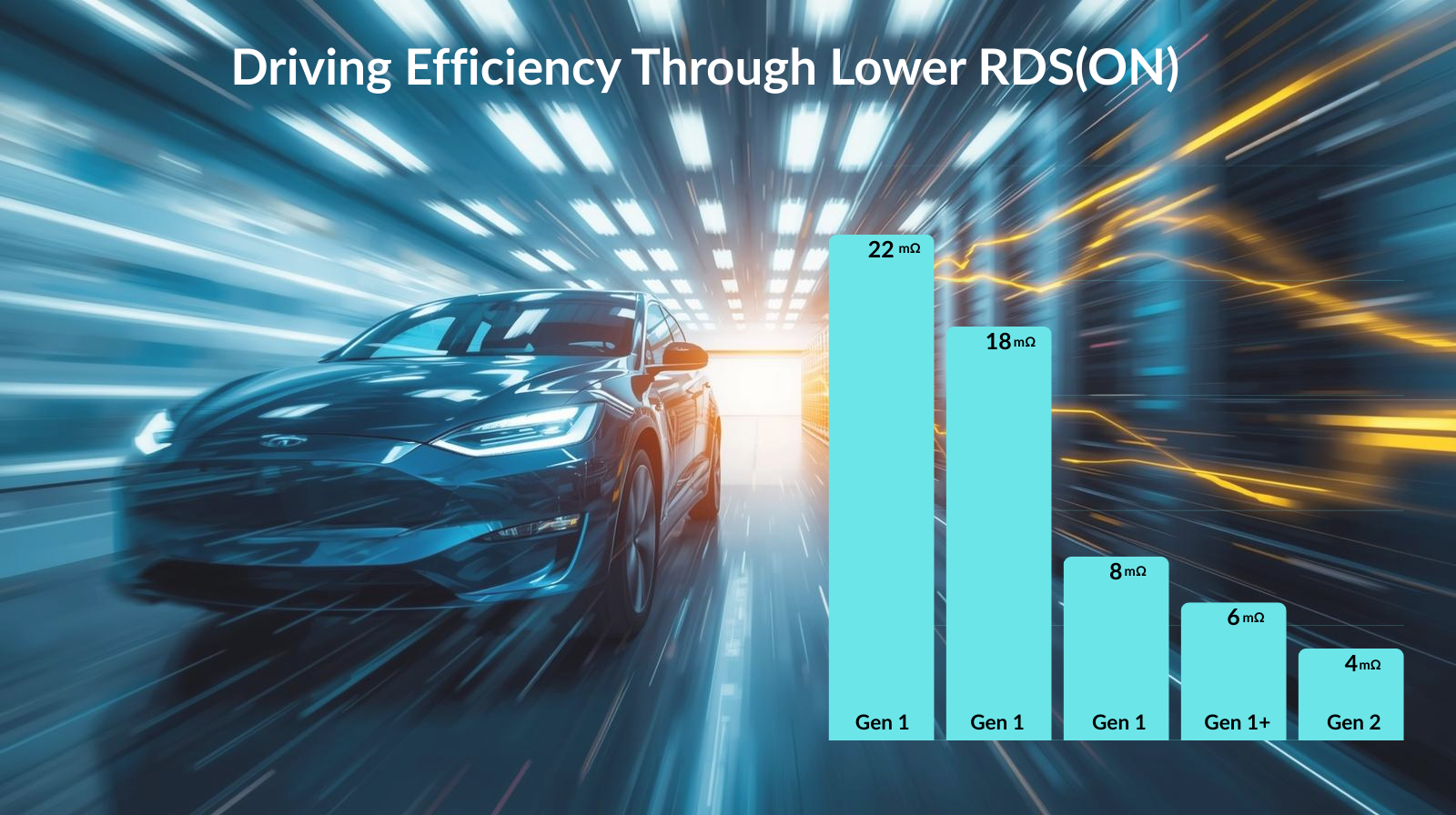
VisIC Technologies, a leader in GaN semiconductor solutions for high-voltage applications, continues to push the boundaries of efficiency and performance in electric mobility and industrial power markets. With the introduction of its first-generation (Gen 1) D³GaN™ 650V devices, followed by Gen 1+, and now second-generation (Gen 2) products, VisIC has created a clear roadmap for achieving maximum energy efficiency through optimized RDS(ON) performance.
Gen 1 – Proven Efficiency
VisIC’s Gen 1 devices established the foundation for GaN adoption in automotive and industrial applications. With RDS(ON) values ranging from 22 mΩ to 8 mΩ, Gen 1 products delivered significant switching speed and efficiency over silicon-based solutions. These devices proved the superior potential of GaN for compact, high-power systems and were the first step toward mass-market adoption.
Gen 1+ – Optimized Performance
To meet growing market demands for higher efficiency, VisIC introduced Gen 1+ devices. By reducing RDS(ON) to as low as 6 mΩ, The 650V Gen 1+ improved conduction losses without compromising switching energy and enabled more power-dense, reliable designs. This generation bridged the gap between the early adoption of GaN and the high-volume needs of automotive OEMs, offering engineers an enhanced balance of efficiency, scalability, and manufacturability. With 98 mm.sq., the GaN bare dice V06DI065R1X13 is one of the biggest dies in the industry to deliver at 650V a current of 170A per device and which makes it ideal to be paralleled inside power modules and deliver power from 50 kW to 150 kW.
Beyond automotive, such performance directly addresses the surging demand for efficient power delivery in AI-driven data center, where massive computing loads require compact, high-efficiency solutions. As a stand-alone GaN die, it provides the power density needed to meet the energy thirst of modern, AI-populated data center while reducing losses and optimizing thermal performance.
Gen 2 – Next-Level Efficiency
VisIC’s 650V Gen 2 devices represent a 33% shrink of die size compared to Gen 1+ and 50% to Gen 1 and is a major leap forward in performance. With RDS(ON) values as low as 4 mΩ, Gen 2 delivers unprecedented conduction efficiency, minimizing power losses and reducing system thermal stress. These D³GaN™ devices are engineered for next-generation EV inverters, on-board chargers, and high-performance power converters, enabling automakers to achieve higher driving ranges, smaller cooling systems, and overall lower system costs. The new high power bare dice V04DI065R2X21 650V/4mOhm can be soldered or sintered on AMB/DBC substrates to increase reliability and performance. With a current capability of 230A the device can be used to increase power density in power modules for EV drive train inverter.
Efficiency by Design
Lower RDS(ON) directly translates to higher system efficiency and reduced energy losses. Across its product roadmap, VisIC demonstrates its commitment to continuous improvement—ensuring that each generation of D³GaN™ devices provides measurable benefits in performance, power density, and total cost of ownership. Both products are today available as bare dice for customer evaluation. Single chip top side cooled TC package will be available before end of the year and VisIC is working on a half bridge power module with parallel dice which will come soon.
“From our first-generation devices to our latest Gen 2 GaN, VisIC has consistently focused on one clear goal: enabling the most efficient power electronics for electric vehicles and industrial applications,” said Tamara Baksht, CEO. “By reducing RDS(ON) with each new generation, we help our customers design systems that are not only more efficient but also more compact and cost-effective.”
Press contact:
Dieter Liesabeths
SVP of Product
Dieter@visic-tech.com
